Introduction to Microprocessor
8085 Microprocessor Definition: When we hear the word microprocessor then what comes to our mind is a small (i.e-micro) IC that can process data i.e.- perform arithmetic and logical operations. The microprocessor reads the instructions from memory and executes them line by line.
As we know that all of this operation is performed generally all of this operation is done by the ALU unit in Microprocessor.
by the CPU in a large computer.
What is the 8085 Microprocessor Kit?
ALU:- This section is used for performing the arithmetic and logical operations in Microprocessor. Here A and B are the input pins where operands are put on which we want to perform arithmetic and logical operation. The a and B sections are operand sections and it processes it according to the given instruction.

Arithmetic operations:- Like addition, subtraction, multiplication, division, etc.
Logical Operation:- Like AND, OR, NOT, EX-OR, etc. all logical operations.
Opcode:- A Binary code that indicates the operation to be performed is called as an opcode.
Operands:- The data on which the operation is to be performed is known as operand.
Instruction:-The combination of an opcode and an operand, that can be used to instruct a system is called an instruction.
Instruction set:- A list of all the instructions that can be issued to a system is called an instruction set.
Program/Subroutine/Routine:- A set of instructions written in a particular sequence, so as to implement a given task. A subroutine in assembly refers to a function as in C/C++.
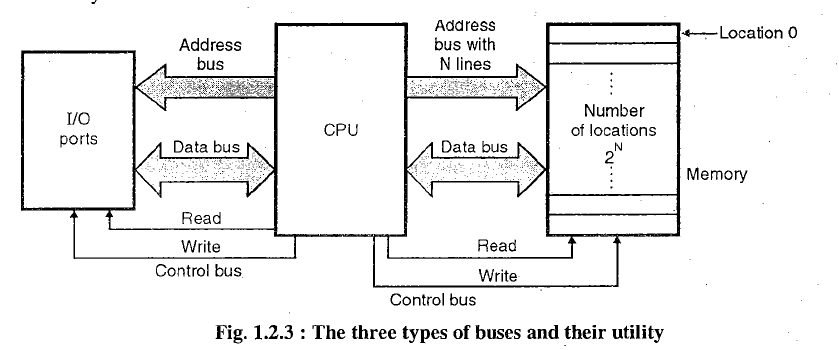
Bus:- A group of lines, pins, or signals having common functions is termed the bus.
There are three buses in the 8085 Microprocessor:
1. Data bus– The Microprocessor has an 8-bit data bus. It carries data(to receive and to transmit) from memory or to memory.
2. Address bus-Microprocessor has a 16-bit address bus. Generally, it is used to select the memory or I/O location through which we want to communicate the microprocessor.
3. System bus– It provides control and timing signals to perform various operation.
Memory:- Generally a memory is used for storage purposes. We can store the data, instruction sets, etc. Instruction sets are stored in memory in the form of binary numbers. It provides that information to the Microprocessor whenever necessary. The microprocessor reads instructions from memory and performs the operation in its ALU section. Results are transferred to the Output Section(LCD display, LED, others). It may also stored in memory as it needs.
There are two types of memory:
RAM(Random Access Memory)- It is a type of memory. it provides both reading and writing facilities.
ROM(Read Only Memory)-Data or programs stored in ROM can only be read. It can not be altered. It doesn’t provide a writing facility.
Pin Diagram and its description
Control And Status Signal:-
S0 and S1:-It is used for the status signal in the microprocessor.
ALE(Arithmetic Latch Enable):-This signal is used to capture the lower address presented on the multiplexed address and data bus.
RD:-This is active low input generally
used for reading operations.
WR:- This is active low input used for writing operations.
IO/M:-This pin is used to select the memory or input-output through which we want to communicate the data.
READY:-As we know memory and input-output have slower responses than microprocessors. So a microprocessor may now be able to handle further data till it completes the present job. So it is in a waiting state. As it completes the present job it sets the READY pin. The microprocessor enters into a wait state while the READY pin is disabled.
RESET IN:- This is active low input. This pin is used to reset the microprocessor. An active low signal applied to this pin resets the program counter inside the microprocessor. The buses are tristated.
RESET OUT: If we want to reset the external devices connected to the microprocessor then a signal applied to this pin resets the external devices.
DMA Request Signal:
HOLD and HLDA:-HOLD is an active high input signal used by the other controller to request microprocessors about the use of address, data, and control signal. The HOLD and HLDA signals are used for direct memory access(DMA). DMA controller receives a request from a device and in turn issues the HOLD signal to the microprocessor.
The processor releases the system bus and then acknowledges the HOLD signal with the HLDA signal. The DMA transfer thus begins.
8085 Microprocessor-Based Stepper Motor Control System
Addressing Modes in 8085 Microprocessor
The 8085 microprocessor has several addressing modes that are used to access memory locations. Some of the most commonly used addressing modes in the 8085 microprocessor are:
The way of specifying data to be operated by an instruction is called addressing mode.
Why use addressing modes in the 8085 microprocessor?
Here are some reasons why addressing modes are used in the 8085 microprocessor:
- Flexibility: Addressing modes provide a flexible way to access data and instructions in memory. Different addressing modes allow programmers to choose the most appropriate addressing technique for a particular task, depending on the type of data being accessed, the size of the data, and other factors.
- Memory optimization: Addressing modes can help optimize the use of memory resources by allowing data and instructions to be accessed in the most efficient way possible. For example, using indirect addressing modes can reduce the amount of memory needed to store addresses, while using indexed addressing modes can reduce the number of memory accesses needed to access a large array of data.
- Performance optimization: Addressing modes can also help to optimize the performance of the microprocessor by reducing the number of memory accesses needed to fetch data or instructions. This can help to speed up the execution of programs and improve the overall efficiency of the microprocessor.
- Reduced code size: Addressing modes can help to reduce the size of code needed to perform a particular task. By using addressing modes that allow data and instructions to be accessed using fewer instructions, programmers can write more compact and efficient code.
There are five types of addressing modes in 8085.
1. Immediate Addressing Mode: – An immediate is transferred directly to the register.
Eg: – MVI A, 30H (30H is copied into the register A)
MVI B,40H(40H is copied into the register B).
2. Register Addressing Mode: – Data is copied from one register to another register.
Eg: – MOV B, A (the content of A is copied into the register B)
MOV A, C (the content of C is copied into the register A).
3. Direct Addressing Mode: – Data is directly copied from the given address to the register.
Eg: – LDA 3000H (The content at the location 3000H is copied to the register A).
4. Indirect Addressing Mode: – The data is transferred from the address pointed by the data in a register to another register.
Eg: – MOV A, M (data is transferred from the memory location pointed by the register to the accumulator).
5. Implied Addressing Mode: – This mode doesn’t require any operand. The data is specified by the opcode itself.
Eg: – RAL
CMP
Advantages of Addressing Modes in 8085 Microprocessor:
- Versatility: The 8085 microprocessor supports several addressing modes, which allows for a wide range of memory access and manipulation options.
- Efficient memory usage: Different addressing modes allow for efficient use of memory, reducing the memory footprint of programs and making the best use of available memory.
- Easy to use: The addressing modes are easy to use, making it simple for programmers to write and execute complex programs.
- Improved performance: The use of different addressing modes can improve the performance of programs, as the correct addressing mode can be chosen to match the specific requirements of the program.
Disadvantages of Addressing Modes in 8085 Microprocessor:
- Complexity: The various addressing modes can be complex, making it difficult for programmers to choose the correct mode for a given task.
- Overhead: The use of different addressing modes can result in additional overhead, as the microprocessor must perform additional operations to access memory.
- Debugging difficulties: Debugging programs that use multiple addressing modes can be difficult, as the programmer must keep track of the different modes used in each memory access.
- Limitations: The addressing modes are limited by the size of the program counter and the memory address space, which can impact the performance of large programs.
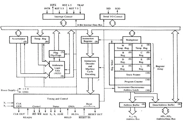
Functional block diagram of the 8085 Microprocessor.
Block Diagram of 8085 Microprocessor.

Acumulator:-It is an 8-bit register that is used to perform arithmetical and logical operations. It stores the output of any operation. It also works as a register for i/o accesses.
Temporary Register:-It is an 8-bit register that is used to hold the data on which the accumulator is computing operation. It is also called an operand register because it provides operands to ALU.
Registers:- These are general purposes registers. Microprocessor consists of 6 general purpose registers of 8-bit each named as B, C, D, E, H, and L. Generally these registers are not used for storing the data permanently. It carries the 8-bit data. These are used only during the execution of the instructions.
These registers can also be used to carry the 16 bits of data by making a pair of 2 registers. The valid register pairs available are BC, DE HL. We can not use other pairs except BC, and HL. These registers are programmed by the user.
ALU:-ALU performs the arithmetic operations and logical operations.
Flag Registers: It consists of 5 flip flop which changes its status according to the result stored in an accumulator. It is also known as status registers. It is connected to the ALU.
There are five flip-flops in the flag register as follows:
1.Sign(S)
2.zero(z)
3.Auxiliary carry(AC)
4.Parity(P)
5.Carry(C)
The bit position of the flip flop in the flag register is:
All of three flip-flops are set and reset according to the stored result in the accumulator.
- Sign- If D7 of the result is 1 then the sign flag is set otherwise reset. As we know a number on the D7 always decides the sign of the number.
if D7 is 1: the number is negative.
if D7 is 0: the number is positive.
2. Zeros(Z)- If the result stored in an accumulator is zero then this flip flop is set otherwise it is reset.
3. Auxiliary carry(AC)- If any carry goes from D3 to D4 in the output then it is set otherwise it is reset.
4. Parity(P)- If the no of 1’s is even in the output stored in the accumulator then it is set otherwise it is reset for the odd.
5. Carry(C)- If the result stored in an accumulator generates a carry in its final output then it is set otherwise it is reset.
Instruction registers(IR):- It is an 8-bit register. When an instruction is fetched from memory then it is stored in this register.
Instruction Decoder: The instruction decoder identifies the instructions. It takes the information from the instruction register and decodes the instruction to be performed.
Program Counter:-It is a 16-bit register used as a memory pointer. It stores the memory address of the next instruction to be executed. So we can say that this register is used to sequence the program. Generally, the memory has 16-bit addresses so it has 16-bit memory.
The program counter is set to 0000H.
Stack Pointer:-It is also a 16-bit register used as a memory pointer. It points to the memory location called stack. Generally, the stack is a reserved portion of memory where information can be stored or taken back together.
Timing and Control Unit:-It provides timing and control signals to the microprocessor to perform the various operations. It has three control signals. It controls all external and internal circuits. It operates with reference to the clock signal. It synchronizes all the data transfers.
There are three control signals:
- ALE- Airthmetic Latch Enable, It provides a control signal to synchronize the components of the microprocessor.
2. RD- This is an active low used for reading operation.
3. WR- This is an active low used for writing operations.
There are three status signals used in microprocessors S0, S1, and IO/M. It changes its status according to the provided input to these pins.
Serial Input Output Control-There are two pins in this unit. This unit is used for serial data communication.
Interrupt Unit-There are 6 interrupt pins in this unit. Generally external hardware is connected to these pins. These pins provide an interrupt signal sent by external hardware to the microprocessor and the microprocessor sends acknowledgment for receiving the interrupt signal. Generally, INTA is used for acknowledgment.
Register Section:-Many registers have been used in the microprocessor.
Difference between address and data bus